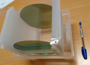
Turbo for electronics? Researchers have succeeded for the first time in making a semiconductor chip from graphene, the basis for fast electronics based on carbon. This is made possible by combining a layer of graphene with silicon carbide, which gives graphene the band gap it needs to be a semiconductor. In initial tests, charges in the excited graphene semiconductor moved ten times faster than silicon, and generated less heat than common semiconductor components, the team reports in “Nature.”
Until now, silicon has been the semiconductor of choice: this element is found in almost all transistors and electronic circuits, where it acts as a switch and amplifier for charge transport. As with all semiconductors, the material's band gap is important: in the normal state, electrons are tightly bound in a semiconductor—it's not a conductor. However, if you add energy in the form of an electric voltage, light, or heat, the electrons jump over an energy barrier—the band gap—and become mobile.
Searching for new semiconductors
However, due to advancing miniaturization and high performance requirements in computer technology, silicon-based electronics are now reaching their limits. So scientists are looking for alternative, more efficient semiconductors. A hot candidate for this is graphene: this material, which resembles a chain link fence made of carbon atoms, is transparent, light, flexible and incredibly stable – but not a semiconductor in nature. It's missing the band gap.
This is where a new development by a team led by Jian Zhao from Tianjin University in China works. They were looking for a way to give graphene its missing band gap and at the same time make practical semiconductor chips. Previous experiments have already shown that graphene's electronic properties can be changed by reducing the range of motion of its electrons — for example, by cutting graphene into narrow bands. However, quality varies greatly.

“Sandwich” made of silicon carbide
So Zhao and his team looked for another method that could be easily scaled up to industrial scale — and found it. The starting point of the process is two thin plates made of silicon carbide (SiC), one side of which consists mainly of silicon atoms, while the other side has the carbon layer of the carbide turned outwards. The wafers are now placed one on top of the other with the carbon and silicon sides facing each other and heated to about 1,600 degrees in an argon atmosphere.
Under these conditions, carbon atoms are released from the carbide layer and deposited on the silicon surface of the opposing material plate. “This graphitic layer that grows on this surface has the lattice structure of graphene, but is partially parallel-bonded with silicon carbide,” Zhao and his colleagues explain.
Graphene has a band gap
Importantly, these bonds change the electronic properties of graphene. A layer of graphene bonded to silicon carbide creates a band gap of about 0.6 electron volts, the team reports. For comparison: the band gap of epigraphene is half as large as the band gap of silicon and close to that of the semiconductor germanium at 0.65 electron volts. As a result of this band gap, graphene requires an energy supply that allows the electrons to cross the energy barrier – making graphene a semiconductor.
“But the big question in our work over the past decade has been: Is this material good enough to work in practice?” says senior author Walt de Heer of the Georgia Institute of Technology in Atlanta. The answer was provided by early experiments where the researchers applied electricity to their inscription plates.
Ten times higher charge mobility than silicon
The result: At room temperature, the excited graphene semiconductor exhibits charge movement of more than 5,000 square centimeters per volt per second. This value indicates how quickly and easily electrons and holes move through the material. As Zhao and his team explain, the conductivity of graphene semiconductors is ten times that of silicon and 20 times that of other two-dimensional semiconductors. “It's more like a highway compared to a gravel road,” de Heer says.
However, graphene has additional advantages over silicon and parallel: “It is very efficient, does not heat up quickly and enables high electron speeds,” explains de Heer. “Now we have a very strong graphene semiconductor, which has higher mobility and other unique properties than silicon.” According to the researchers, this opens up new possibilities for making electronic components more efficient and faster. “For me, it's as much a milestone in aviation as the Wright brothers,” says de Heer.
This is how researchers turned graphene into a semiconductor.© Georgia Institute of Technology
However, graphene semiconductor chips and circuits still need to be improved until there are practically usable graphene-based transistors. Nevertheless, the researchers see significant commercial potential in their graphene-silicon carbide chips. They are useful, for example, in high-performance electronics, space travel, and biomedical devices. (Nature, 2023; Two: 10.1038/s41586-023-06811-0)
Quelle: Georgia Institute of Technology
January 4, 2024 – Nadja Podbregar